The use of good ECAD is crucial to the design and development of high-quality electronic products. ECAD can provide a variety of benefits, such as reduced design cycle time and error minimization.offer various benefits, reduced design cycle time, and
One essential aspect of ECAD, which I consider critical,Among the many important aspects of ECAD, I consider checking the trace impedance to be the most critical.
For example, let's look at how routing a few traces can cause unexpected issues.
First, let's look at an example of how to check for accidental errors in a design.
Several years ago, I designed an RF front end based on the RF2052.
The RF2052 is an RF Mixer with a RF2052 is an RF mixer with a frequency synthesizer. Frequency ranges from 30 MHz to 2.5GHz.
In my opinion, this chip gives excellent performance in designing low cost spectrum analyzers. A tool like RF Explorer, for example, uses the RF2052 in its front end.
When you use a chip like this, it's extremely important that the RF path maintains a constant impedance.
As an example, let's say I want to verify the impedance of a specific track.

FIG.1 RF Front end of a low cost RF analyzer (designed by myself)
Assume we want to analyze the trace between Balun B1 and U1's RF input.
We can do this by asking our CAD to create a trace with a specific impedance.
Despite this, there are some parts of our design that simply cannot be done due to physical reasons. If this happens, how far are we from our desired impedance, and does it matter?
I have started using an ECAD tool called ANSYS Slwave. A Signal Integrity tool like this can be extremely useful when we analyze our board both from a signal integrity point of view as well as from an EMC viewpoint.
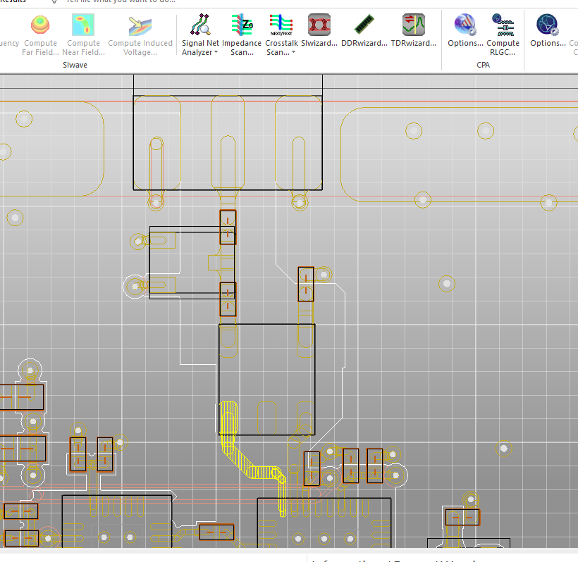
Let's say I want to analyze the above trace, all I have to do is import the project to ANSYS and select the trace.
After clicking Signal Net Analyzer, I see the results

FIG2. Using AnSys Slwave I can check any trace.
The impedance of the trace changes over engthh as I travel along it, according to AnSys.
As an example, the impedance dropped from around 75 ohm near the Balun to around 59 ohm Near the RF2052. What an amazing piece of information!

FIG.3 how the impedance change over the trace.
Let's see more traces.

FIG.4 looking at my design more traces
I can see some traces are correct, while others suffer of some deviations during the tracking.
For example the Net called NetR18-2 has in 2 parts 2 changes of impedance. Let's see why.
Using Altium I look for NetR18-2 and I see

FIG.4 We have 2 change of impedance, since we are going from the top layer to the bottom layer.
In my opinion, this is one of the best methods that can help me minimize errors in my design, so I decided to share it with you so that all of us could benefit from it. There is so much more we can do with AnSys than that. For instance, we can estimate the crosstalk between traces, or we can simulate a TDR simulation on a particular trace in order to estimate the crosstalk.
Among all the tools I have tried, the one I like most is called the EMI scanner. Since I do a lot of work helping companies with their EMC compliance, the near field emission from some traces is very important to me since I do a lot of work for them. Please do not hesitate to contact me if you would like to know more about this.
Comments