Emissions due to insulated power supply
- Francesco Poderico
- Jan 29, 2024
- 3 min read
As a matter of fact, it is quite common these days that we need some amount of insulation between our electronics and the outside world. If you had designed a PoE product, for example, you would typically have an insulation of 1.5kV in your product.
In most cases, the insulation voltage is determined by the applicable safety standard that governs the product.
Nevertheless, when you use an insulated DCDC converter, you should be aware that three main mechanisms can make your product very noisy from the perspective of the EMC. These emissions may range in frequency from a few hundred of kHz up to hundreds of MHz, with a few exceptions.
Having said that, the mechanism of the emission is different, and I would like to offer a discussion of these three different mechanisms today.
EMC emission mechanism below 80 MHz
The EMC emission in the lower spectrum band of a DCDC converter is very similar to what I have already discussed here: https://www.emcdesignsolutions.com/post/common-mode-coupling-mechanism-on-ac-dc-converter

Although the "cure" is similar to the emission path, it differs slightly.
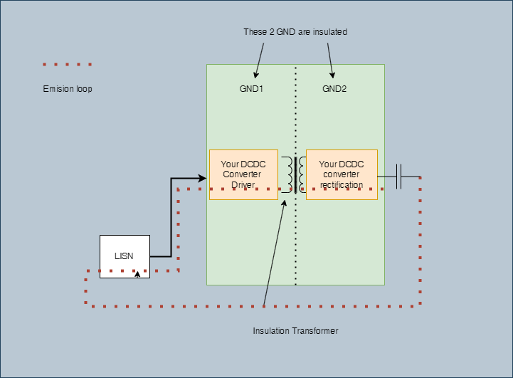
Below is a sketch of a typical emission path during a CE test. This applies to AC/DC as well as DC/DC converters, with some differences, for example, the position of the LISN it is usually on the floor for AC-powered equipment and on the table for DC-powered equipment. Check out the standards for more information on the setup
Normally, your equipment will be set up on a wood table that will be 80 centimeters above the floor and 80 centimeters away from the chamber. The chamber is conductive and the distance between the horizontal and vertical sides of the chamber is very important to ensure that repeatable measurements can be made between different EMC testing laboratories.
Now, if you look at the drawing, you will see that I have drawn a capacitor in it. It is the parasitic capacitor between the vertical and horizontal planes of the chamber and your electronic board that gives you issues, since it creates the current loop I have sketched.
The bigger the capacitor, the higher the emission.
It is impossible to control the value of that capacitor.
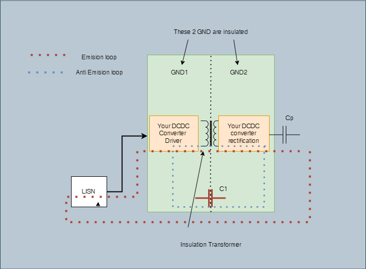
How can we stop the emissions? Here is the next diagram.
Let's create the Antiemission loop!
Let's add a capacitor C1 between the 2 insulated GND (GND1 and GND2 in the sketch).
.

For the moment, let's assume that C1 is greater than Cp.
In this instance, C1 is a Y capacitor that sits between the "input GND" and the "output GND". I have named them GND1 and GND2 in the sketch, but in reality, they are both GNDs.
If C1 > Cp, which should be quite easy to achieve, then it would appear that there will be a reduction in the amount of common mode emissions that cross the LISN, as I said if C1 >> Cp. There will be less and less emissions as a result, and consequently, the emission level will be lower.
There are, however, a few limitations.
You need a Y-capacitor
It is usually a "big" capacitor
You should check your standard to see the leakage limit for your application since the higher the capacitor, the greater the leakage current.
Unfortunately, EMC and safety don't always go hand in hand, and passing emissions sometimes creates safety issues, so I suggest you use a smaller power capacitor if you can.
It is my hope that you have found this useful. I will explain the next 2 mechanisms in my next post, which usually occur above 100 MHz.
The first mechanism uses the cables to emit.
The second mechanism uses any metal (including your enclosure) as patch antenna to emit.
See you next time.
Don't forget to like and follow me if you enjoy.
Comments