EMC issues due to optoisolators.
- Francesco Poderico
- Nov 27, 2022
- 2 min read
EMC is considered by many to be a "black magic" for a number of reasons. In some cases, it may be the case that you obtain unexpected emissions from components you were not expecting to have.
Oftentimes, the problem lies in the fact that we tend to ignore what we call "parasitic components" such as the parasitic capacitances and inductances of the components they belong to.
The failure to take care of this can unfortunately lead to unexpected EMC problems in the future.
Would you expect that an optoisolator would have some EMC issues as well? If your answer is No! Then keep reading.
In the course of my work this year, I was involved in a product that had a number of optocouplers between the printed circuit board and an external device.
The design was not fully ready for compliance, and the optoisolator was driven incorrectly as well. Each optoisolator was driven by a microcontroller, and the microcontroller was on a different board (within the same product).
The optoisolators controlled some relays. These relays had some external cables, and they were emitting above the limits.
How is this possible?
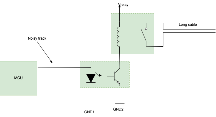
Let's see the following diagram:

A simple circuit like this may fail EMC if you are not careful!
We have a microcontroller on PCB 1, and using an internal connection, we drive a few optoisolators on PCB 2. The optoisolators drive a few relays.
To understand how a simple design like this can emit above the limits we need to study the emission path.
Who is the "real" source of emissions? Probably it is the microcontroller.
During the EMC test, a nearfield probe can be used to verify this. For this kind of troubleshooting, I use a magnetic near-field probe. As soon as I have proved that the source of the emission is the microcontroller, I need to find the path by which the emission is coming from.
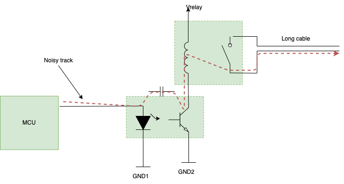
Please see the following diagram, which includes even the parasitic capacitance between the optoisolators.
Can you see now how some of the "local EMI emission" might find its way to the output cable?

The parasitic capacitance of the Opto works as a bridge for the HF signal.
The parasitic capacitor across the optoisolator acts as a bridge for the AC path of the EMI source. In this case, the signal, when it arrives at the relay coil, finds easily its way to the cable, which is the antenna, and therefore the emissions were so high as a result.
What can we do to make sure that doesn't happen in the future?
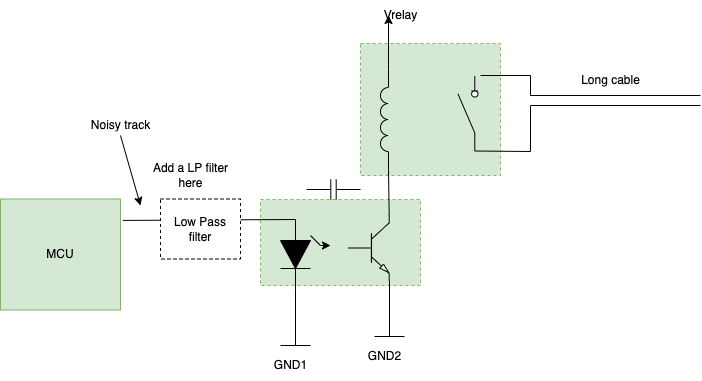
Easy as pie! Each input of the optoisolator should be filtered with a low pass filter. I would like to remind you to keep in mind that if the PCB is not properly laid out (missing GND plane), even the GND pin of the Opto is potentially a source of emission, and it should be treated accordingly.

By adding a low pass filter we can fix all our EMC issues!
Thank you for reading!
Comments