PCB Crosstalk and how to use the ground plane to minimise it.
- Francesco Poderico
- Nov 11, 2022
- 1 min read
To avoid EMI and crosstalk on both PCB traces and connectors, it is crucial to understand the return path current.
Previously, I discussed how a ground plane reduces EMC problems (both emission and immunity). In addition to minimising crosstalk, a ground plane helps minimise interference. You know I believe you don't know a subject well if you can't explain it using a simple example. Therefore I'll explain this using just words and not formulas. If you want to dig into the matter, let me know in the comments, and I'll suggest a few books.
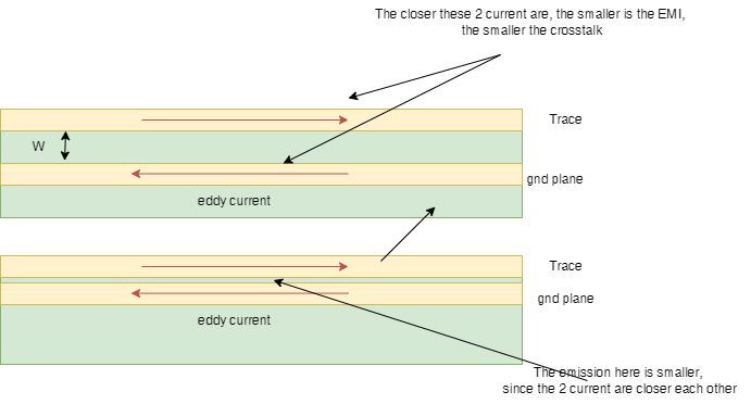
I made this drawing for you to see. Eddy currents are generated when a current is carried on a trace by the ground plane underneath it. This is well known, and I have discussed this already.
Magnetic fields will be created in opposite directions by these two currents.
You can see that in the second drawing (bottom), the two currents are closer together and, as a result, we should expect a weaker magnetic field than in the first example.
Consider a case where w=0 and both currents overlap, in which case there is no magnetic field created.
As a result, the smaller the ground plane, the lower the magnetic emission, and therefore, the lower the crosstalk.
This kind of design detail is essential these days when we have microcontrollers, sensors, FPGA, DDR, etc., on the same board. Minimising the crosstalk between traces is vital today, and understanding your tools is very important.
So... to recap... a ground plane not only improves the radiated emission, radiated immunity, conductive emission and conductive immunity but also has a crucial role in reducing the crosstalk between traces.
I hope you enjoyed it.
Comments